Fabrication process of BiCMOS technology
BiCMOS Logic:
Bicmos technology is a complex processing technology that gives NMOS and PMOS advances amalgamated each other with the upsides of having extremely low power utilization bipolar innovation and high speed over CMOS innovation. MOSFETs give high input impedance logic gates and bipolar semiconductors give high current increase.
Steps for BiCMOS Fabrication:
BiCMOS manufacture process is similar of creation of BJT and CMOS, but only variety is an acknowledgment of the base. The following steps shows the BiCMOS manufacture process
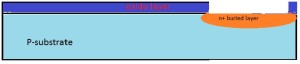
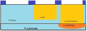
Step1: P-Substrate is taken as shown in the below figure

Step2: P-substrate is covered with the oxide layer

Step3: A little opening is made on the oxide layer

Step4: N-type impurities are heavily doped through that opening
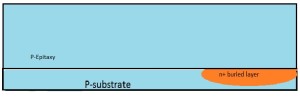
Step5: The P – Epitaxy layer is grown on the whole surface
Step6: Again, whole layer is covered with the oxide layer and two openings are made through this oxide layer.
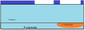
Step7: From the openings made through oxide layer n-type impurities are diffused to shape n-wells
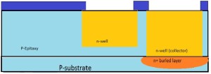
Step8: Three openings are made through the oxide layer to form three active devices.
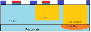
Step9: Gate terminals of NMOS and PMOS are shaped by covering and designing the whole surface with Thinox and Polysilicon.
Step10: At that point P-impurities are added to shape the base terminal of BJT and comparative, N-type impurities are vigorously doped to producer emmiter terminal of BJT, source and channel of NMOS and for contact reason N-type impurities are doped into the N-well collector.
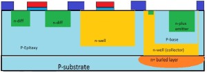
Step11: To form source and drain regions of PMOS and to make contact in P-base region the P-type impurities are heavily doped.
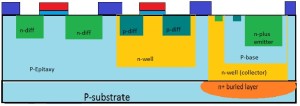
Step12: Then the whole surface is covered with the thick oxide layer.
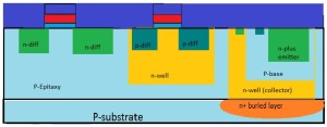
Step13: Through the thick oxide layer the slices are designed to frame the metal contacts.
Step14: The metal contacts are made through the slices made on oxide layer and the terminals are named as appeared in the below figure.
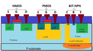
Manufacture of BICMOS is appeared in the above figure with a combination of NMOS, PMOS and BJT. In the manufacture cycle a few layers are utilized, for example, channel stop implant, thick layer oxidation and guard rings.
The creation cycle will be hypothetically hard for including both the advancements CMOS and bipolar. Parasitical bipolar semiconductors are delivered incidentally is an issue of manufacture while handling p-well and n-well CMOS. For the creation of BiCMOS numerous extra advances added for adjusting of bipolar and CMOS parts. Henceforth, the expense of complete manufacture increments.
Channel stopper is embedded in semiconductor devices as appeared in the above figure by utilizing implantation or diffusion or different strategies to restrict the spreading of channel region or to evade the arrangement of parasitic channels.
The high impedance hubs assuming any, may cause the surface leakage currents and to stay away from the progression of current in spots where the current stream is confined these guard rings are utilized.
References:
https://www.iue.tuwien.ac.at/phd/puchner/node48_app.html
https://en.wikipedia.org/wiki/BiCMOS
https://www.brainkart.com/article/BiCMOS-Technology-Fabrication_13173/
Author: Priti Arya


Useful information👍
ReplyDeleteThank u😊
DeleteUseful and innovative information 👍
ReplyDeleteVery important points were mentioned and very useful
ReplyDeleteUseful points are mentioned
ReplyDeleteWell described each n every point 👍
ReplyDeleteUseful information and well described 👍
ReplyDeleteThank u
DeleteUseful information
ReplyDeleteThank u
DeleteSuch a great explanation,,as a very useful info.
ReplyDeleteUseful info
ReplyDeleteInformative👍👍
ReplyDeleteUseful points are mentioned.
ReplyDeleteUseful points are mentioned.
ReplyDeleteVery much important points are mentioned here👍👍
ReplyDeleteVery good information...well described each n every point 👍
ReplyDeleteThank you
DeleteVery good information...well described each n every point 👍
ReplyDeleteThank u for reading our blog.
DeleteVery well explained topic..
ReplyDeleteWell described...keep it up👍
ReplyDeleteThank u
DeleteVery well explained..keep it up
ReplyDeleteUseful information..great 👍
ReplyDeleteThank u for ur feedback
DeleteGreat... 👍
ReplyDeleteThank u
Delete👍👍 great informative
ReplyDeleteThank u
DeleteWell described each point
ReplyDeleteThank u
DeleteVery nice explaination 👍👍👍👍👍👍👍
ReplyDeleteInformative
Thank u
DeleteExplained in a very simplex manner.... Nyc... 👌👍🏻
ReplyDeleteThank you
DeleteNice content 🙌
ReplyDeleteGood One👍
ReplyDeleteVery informative ��
ReplyDeleteInformative��
ReplyDelete👍👍
ReplyDeleteWell described
ReplyDeleteAs well notable infotmation 💯🙌
Thank u
Delete👏🏻👍🏻
ReplyDeleteWell described 👍
ReplyDelete👍👍
ReplyDeleteGood information
ReplyDeleteThank u
DeleteNice described..👍👍
ReplyDeleteNice one and well described ...well done👍🏻
ReplyDeleteNicely explained
ReplyDelete👌👌👏well described
ReplyDeletegood one
ReplyDeleteWell described
ReplyDeleteUseful information
ReplyDeleteVery useful
ReplyDeleteThank u
Delete����
ReplyDeleteWell explained..Good Job ��
ReplyDeleteWell written
ReplyDeleteWell explained..
ReplyDeleteWell described...Nd useful info
ReplyDeleteThank u for your response
DeleteNice one and well described
ReplyDeletewell done👍🏻
Thank u
DeleteWell described and neatly explained. Really helpful..keep it up 👍👍
ReplyDeleteThank you
DeleteGreat
ReplyDeleteWell described
ReplyDeleteWell done 👍
ReplyDeleteNice content ��
ReplyDeleteUseful information about new innovation👍
ReplyDeleteThank u
Deletewell described 👍 Nice content .
ReplyDeleteThank u
DeleteInformative
ReplyDeleteVery Informative
ReplyDeleteThank you
DeleteImpressive work ��
ReplyDeleteThis comment has been removed by the author.
ReplyDeleteThis comment has been removed by the author.
ReplyDelete👍 Nice blog
ReplyDeleteWell explained with proper info with steps and advantage as well... good work👍
ReplyDeleteThank u
DeleteGood Job 💯
ReplyDeleteGreat 👍
ReplyDeleteVery informative
ReplyDeleteThank you
DeleteWowwww nice content
ReplyDeleteThank u
DeleteVery informative💯
ReplyDeleteThank you
DeleteInformative 👌
ReplyDeleteVery well explained, good job !!
ReplyDeleteThank u for ur feedback
DeleteWell explained 👍
ReplyDeleteUseful information
ReplyDeleteWell done, explanatory details are very useful 👍
ReplyDeleteThank u
DeleteNice
ReplyDeleteUseful information
ReplyDeleteThank you
DeleteInformative
ReplyDeleteThank you
DeleteGreat job!
ReplyDeletegreat content!!
ReplyDeleteThank you
DeleteGreat content
ReplyDeleteGood information
ReplyDeleteThank u😊
DeleteThis comment has been removed by the author.
ReplyDeleteVery well presented and it is very informative.
ReplyDeleteThank you
DeleteWell explained....keep it up
ReplyDeleteThis comment has been removed by the author.
ReplyDeleteWell explained.
ReplyDeleteExtremely informative!!
ReplyDeleteExcellent information...nice job guys..keep it up!!!
ReplyDeleteThank you
ReplyDeleteVery nice �� keep it up
ReplyDeleteNice Blog
ReplyDelete