Posts

App Engine

Image
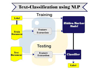
The process of splitting written text into meaningful components, such as words, sentences, or phrases, is known as text segmentation. Natural language processing refers to both the mental processes that humans utilise when reading text and the artificial processes that are implemented in computers. This blog describes how text segmentation can be performed with the help of  Hidden Markov model(HMM) Natural language processing (NLP)  challenges are where naive Bayes are most commonly utilised. Naive Bayes predicts a text's tag. They calculate each tag's probability for a given text and output the tag with the highest probability.         In Naive Bayes, we calculate the probability of label y using the joint probability, assuming that the input values are conditionally independent. Because letter or word sequences are dependent, this assumption does not hold true in the text segmentation problem. We present a parameter-free text segmentation approach b...

Bicmos Inverter

Image
  BICMOS INVERTER:- A simple BiCMOS inverter can be constructed from a pair of MOS transistor and NPN transistors. Each of the MOS transitors are cascaded with an NPN transistor. When the input is HIGH, the NMOS transitor is conducting becoming the base current for the Q2 NPN transistor causing the discharge current to drop. Conversely when the input is LOW, the PMOS transistor is conducting becoming the base current for the Q1 NPN transistor, causing the output the increase. The inverter has low input impedance and low output impedance. The inverter has high current driving capability, occupies smaller area and has high noise margins. Output voltage swing should be reduced for a better performance of BiCMOS circuit.                                                                       fig1-Bicmos Inverter Cir...

Bicmos technology

Image
  BICMOS Technology   What is BiCMOS Technology? While the whole semiconductor industry is excited about FinFET and FDSOI processor technologies, there is one semiconductor technology that considered by engineers as "the process for real men" and its called BiCMOS. This  is one of the major semiconductor technology and is a highly developed technology. BiCMOS technology combines Bipolar and CMOS semiconductors in a single integrated circuit. By holding the advantages of Bipolar and CMOS , BICMOS is able to accomplish VLSI circuits with speed-power-density performance previously unattainable with either technology individually.                                     BiCMOS CME8000 The figure shown is the first  analog/digital  receiver IC and is a BiCMOS integrated receiver with very high sensitivity. Advantages of BiCMOS technology: Since it is a combination of bipolar an...

Bipolar technology

Image
  Bipolar Technology: Bipolar transistors are part of integrated circuits and their operation is based on two types of semiconductor material or relies on both types of charge carriers holes and electrons. These are generally classified into two types as  PNP and NPN , grouped based on doping of its three terminals and their polarities. Bipolar transistors affords high switching as well as input/output speed with good noise performance. It can switch direct current or function as an oscillator .  Physically, a bipolar transistor amplifies current , but it can be connected in circuits designed to amplify voltage or power. Bipolar devices can switch signals at high speeds, and it can be manufactured to deal with large currents so that they can serve as high power amplifiers in audio equipment and in wireless transmitters. Bipolar devices are not particularly effective for weak signal amplification, or for application, or for applications requiring high circuit impedance....

CMOS technology

Image
  CMOS Technology: The term CMOS stands for “Complementary Metal Oxide Semiconductor”. This is one of the most popular technology in the computer chip design industry and it is broadly used today to form  integrated circuits  in numerous and varied applications. Today’s computer memories, CPUs, and cell phones make use of this technology due to several key advantages.  This technology makes use of both P channel and N channel semiconductor devices. One of the most popular MOSFET technologies available today is the Complementary MOS or CMOS technology. This is the dominant semiconductor technology for microprocessors, microcontroller chips, memories like RAM, ROM,  EEPROM and   application-specific integrated circuits (ASICs). CMOS CD74HC4067 The figure shows the utilization of CMOS technology in manufacturing the digital controlled switch devices. Advantages The advantages of CMOS include the following. The main benefits of CMOS over TTL are good noise...

Fabrication process of BiCMOS technology

Image
  BiCMOS Logic: Bicmos technology is a complex processing technology that gives NMOS and PMOS advances amalgamated each other with the upsides of having extremely low power utilization bipolar innovation and high speed over CMOS innovation. MOSFETs give high input impedance logic gates  and bipolar semiconductors give high current increase. Steps for BiCMOS Fabrication:  BiCMOS manufacture process  is similar of creation of BJT and CMOS, but only variety is an acknowledgment of the base. The following steps shows the BiCMOS manufacture process Step1:   P-Substrate is taken as shown in the below figure P-substrate Step2:   P-substrate is covered with the oxide layer P-substrate with oxide layer Step3:  A little opening is made on the oxide layer Opening is made on the oxide layer Step4:  N-type impurities are heavily doped through that opening N-type impurities are intensly doped through the opening Step5:  The P – Epitaxy layer is grown ...